
| Here is an example of how a circuit is implemented on a cell matrix. The process starts with a precise description of the desired circuit logic. Below we show one type of description, a schematic diagram. Schematic diagrams show the gates used, and how they are hooked up to create the desired circuit. | |
| This particular circuit is a simple arithmetic logic unit, or ALU. ALUs perform simple functions on their inputs and are commonly used onboard computer CPUs to speed up the execution of a predetermined set of mathematical calculations or other functions seen often in the execution of software programs. Using reconfigurable hardware like a cell matrix, that set of functions could be changed on the fly based on what functions are most needed for the software that is currently running. | |
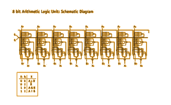
Schematic Diagram of an 8 bit, 4-function arithmetic logic unit. (Click here for a larger, more legible version of this image.) |
|
| This ALU takes in two 8 bit numbers, one labelled A and one labelled B, and performs one of four functions on its inputs. Each of the bits of A is shown fed in through the top, on the wires labelled A0 to A7. B is fed in through the bottom, on the wires labelled B0 to B7. At the bottom you will also see wires labelled X0 to X7: X is the output of the ALU, available once a function is applied to A and/or B. The functions this circuit can perform on A and B are listed in the box in the lower right. This information is also available from studying the schematic diagram in detail and following various inputs and combinations through the paths they take. The circuit can add A to B, or logically AND or OR the bits of A and B, or it can return A with all its bits flipped (sometimes called inverting A). Which function the circuit performs is dictated by two additional inputs, f0 and f1, which are fed in from the left on the schematic diagram. | |
| A schematic diagram is just a circuit specification: it is not a physical circuit. The next step toward a physical circuit is to translate the specification to a specific type of hardware. The next figure shows one way to create the desired ALU circuit on a cell matrix. The matrix shown here is made up of a set of contiguous two dimensional, four-sided cells, which looks like a grid of squares in this figure. Each square is a cell. No other hardware is used besides cells: the wires and gates alike are created using cells. | |
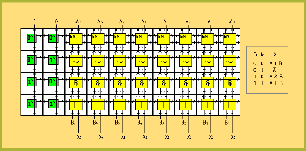
An implementation of the 8 bit ALU on a set of cell matrix cells. Click here for a larger, more legible version of this image. |
|
| The bits of the numbers A and B are fed in from the top and bottom, as they were in the schematic diagram, and X is retrieved from the bottom of the circuit. Each row of the matrix is dedicated to a different function f. The first to (f1,f0) = (0,0), the second to (0,1), and so on. The rest of the matrix is set up similarly to the schematic: A and B are passed to each of the four combinatorial logic blocks needed for each of the four functions. All four functions are performed on the input, with one of the four results selected for output into X. | |
| This is still just a diagram, not a physical circuit. The way to build a working circuit from this diagram is to set the memory, or lookup table, in each cell. One can enter each of these memory settings onto a physical cell matrix, or onto the cell matrix simulators we provide on this site, and end up with a working circuit. A file is provided in the downloads section that loads in the memory settings automatically. You can load this file into the PC-based cell matrix simulator. | |