
| Here is an example of how a circuit is implemented on a cell matrix. The process starts with a precise description of the desired circuit logic. Here we show one type of description, a schematic diagram. Schematic diagrams show the gates used, and how they are hooked up to create the desired circuit. The circuit diagrammed here is a small memory circuit, containing sixteen four-bit values, or "words." | |
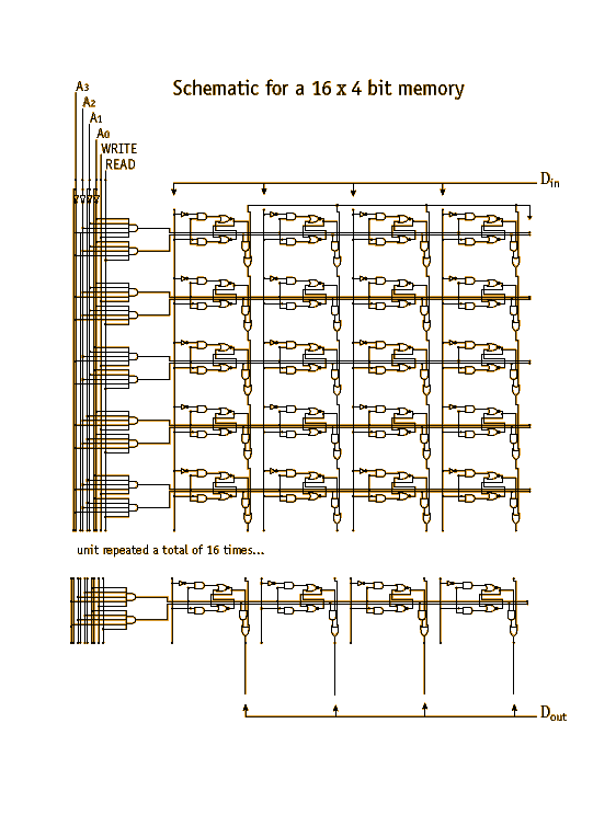
Schematic Diagram of a 16 by 4-bit memory circuit. (Click here for a larger, more legible version of this image.) |
|
|
The memory's bit storage is the bulk of the area of the circuit, on the right, consisting of storage circuits made of flip flops, along with other logic that provides a way to get and set the bits held in the flip flops. Each row holds a 4-bit word.
The set of four wires on the upper left, labelled A0 to A3, provide a mechanism to uniquely access each of the rows in the memory. This is generally called addressing the memory, and the four bits are usually called the address. Four bits permit 16 distinct addresses, and thus this circuit has 16 rows of words. Not all are shown. The other two lines in the upper left, READ and WRITE, indicate whether the memory address should be used to read out the memory contents at that address (READ) or put a new value into the memory at that row (WRITE). The four input lines are shown at the top, labelled collectively Din. These lines permit a new value to be entered into any of the rows. In a complementary role, the four output lines, labelled Dout, permit an existing memory value to be read out of any row of the memory. Note that the Din and Dout lines are shared by all memory rows, and the coordination of which row is reading or writing those lines is handled by the address bits. |
|
| A schematic diagram is just a circuit specification: it is not a physical circuit. The next step toward a physical circuit is to translate the specification to a specific type of hardware. The next figure shows one way to create the desired memory circuit on a cell matrix. The matrix shown here is made up of a set of contiguous two dimensional, four-sided cells, which looks like a grid of squares in this figure. Each square is a cell. No other hardware is used besides cells: the wires and gates alike are created using cells. | |
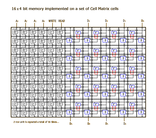
An implementation of the memory schematic diagram on a set of cell matrix cells. Click here for a larger, more legible version of this image. |
|
|
The righthand section is the memory storage, just as it was in the schematic, and the lefthand section is the addressing and read/write determination logic. Each memory row takes 2 rows of cells. The cell matrix circuit definition also uses flip flops to store the bits, just as the schematic diagram did. Flip Flops are indicated as boxes labelled 'f.' The boxes labelled 'g' handle the D lines and the read-in or write-out of the bit stored at that location.
Note that in both the schematic and the cell matrix circuit specification, each row address is hard-wired, But it is implemented slightly differently. In the schematic diagram, addressing is done by providing wires for each bit and for its inverse, providing a total of 8 wires, and then an AND gate is set up to tap off of either the Ai wire or the ~Ai (inverse) wire. If you follow the taps carefully, you will see that the first row, for example, the output of the AND gate is one only if all the bits of A equal zero, or an address of (0000). In the cell matrix circuit, each bit is compared to the bit expected for that address, and the results of these comparisons are bitwise ANDed from left to right, accumulating a result. It is important to understand that this happens as fast as it can, at propagation delay speeds, rather than through clocked, synchronized communications. There is no state involved in the transmission of information from one set of logic to the next, and it happens immediately and continuously. Notice also that there are many outputs on the right side of the circuit that aren't being used for anything here. These make it easy to add more bits to the memory. If you want to implement a larger memory, you simply determine how to expand this circuit. Additional address bits can be achieved by adding columns to the address region, and the memory can be enlarged with rows and columns to the bottom and right. This is another cool feature of cell matrices; circuits can be expanded or moved within a matrix simply by swapping or adding memory configurations. |
|
| This is still just a diagram, not a physical circuit. The way to build a working circuit from this diagram is to set the memory, or lookup table, in each cell. One can enter each of these memory settings onto a physical cell matrix and end up with a working circuit. One can simulate this process by setting up cell memories in the cell matrix simulators we provide on this site and then experimenting with the resulting simulated circuit. A smaller memory circuit is provided for you to load into the PC-based cell matrix simulator. | |