The Cell Matrix: An Architecture for Nanocomputing
by
Lisa J. K. Durbeck*, Nicholas J. Macias*
Cell Matrix Corporation
*{ldurbeck|nmacias@cellmatrix.com}
This is a draft paper for the Eighth Foresight Conference on Molecular Nanotechnology.
The final version has been submitted for publication in the special Conference issue of Nanotechnology.
Abstract
Much effort has been put into the development of atomic-scale switches, and more recently toward the construction of computers from atomic-scale components. A larger goal is the development of an atomic-scale universal assembler, which could construct any electronic circuit, not just a specific CPU. We propose the insertion of a level of indirection into the process of constructing these specific or general builders. Rather than building physically heterogeneous systems that implement various digital circuits, we propose that the builder construct physically homogeneous, undifferentiated hardware that is later, after manufacture, differentiated into various digital circuits. This achieves the immediate goal of achieving specific CPU and memory architectures using atomic-scale switches. At the same time, it achieves the larger goal of being able to construct any digital circuit, using the same fixed manufacturing process. Moreover, this opens the way to implementing fundamentally new types of circuits, including dynamic, massively parallel, self-modifying ones. Additionally, the specific architecture in question is not particularly complex, making it easier to construct than most specific architectures.
We have developed a computing architecture that fits this more attainable manufacturing goal. We have also been developing the extra step introduced into the process, that is, taking undifferentiated hardware and differentiating it efficiently and cheaply into desirable circuitry.
The architecture presented here is physically simpler than a CPU or memory or field-programmable gate array. All system function is represented within the atomic unit of the system, called a cell. This unit is repeated over and over to form a multidimensional matrix of cells. In addition to being general purpose, the architecture is highly scalable, so much so that it appears to provide access to the differentiation and use of trillion trillion switch hardware. This is not possible with an FPGA architecture, because its gate array is configured serially, and serial configuration of trillion trillion switch hardware would take years. This paper describes the cell in detail and describes how networks of cells in a matrix are used to create small circuits. It also describes a sample application of the architecture that makes beneficial use of high switch counts.
Introduction
The architecture described here is a general purpose computing platform that gives fine grained control over the design and implementation of digital circuits. It is called the cell matrix architecture. It supports a one-problem, one-machine model of computing, in which the algorithm and circuitry are designed together from first principles, even down to the gate level if desired. Yet this architecture does not require the construction of a universal nanoassembler (Bishop, 1996) to achieve the one-problem, one-machine model. This is because the physical structure of the hardware is in all cases fixed. It consists of a multidimensional array of interconnected processing elements whose behaviors are specified by a changeable memory incorporated into each element. This provides hardware that is "reconfigurable" based on the problem at hand, like field programmable gate arrays (FPGAs). Not only is the physical structure of a cell matrix fixed, but it is completely homogeneous. This is not true for reconfigurable devices in general; however, the cell matrix architecture is one in which all necessary function, including the ability to reconfigure the hardware, is represented within the single repeating structural unit, a cell. Unlike FPGAs, CPUs and memory devices, there are no superstructures or specialized structures within a cell matrix, just identical cells. A cell is a simple structure, consisting of less than 100 bytes of memory and a few dozen gates, as well as wires connecting the cell to its nearest neighbors. The design of a cell and a matrix of cells is described below. The implication is that, once the capability exists to construct a single, structurally simple cell, as well as the capability to connect cells to their neighbors, then, by repeated application, an entire matrix can be built or grown. The matrix can then be used for the construction of any of a wide variety of digital circuits and systems, such as specific CPU and memory designs, parallel processors, multiprocessors, and so on.
In addition to providing a simple physical structure upon which complex computing systems can be created, the cell matrix architecture provides the means to efficiently utilize extremely large numbers of switches, because the complexity of controlling the system does not increase with switch count. Rather, system control increases as cell count increases. The architecture's fine-grained, distributed, internal control permits users to distribute problems spatially rather than temporally. This ability is particularly applicable to large but naturally parallel problems such as searching a large space for an answer, as is needed for detecting chemical signatures (such as those for cancer), decrypting text, and root finding for mathematical functions of the form f(x) = n. On a sequential CPU/memory machine these problems are distributed temporally, as the elements of the search space are dealt with one by one until an answer is found. In a spatially distributed machine algorithm, the process of analyzing one search space element can be replicated across a large matrix of processors, each of which searches its small portion of the search space. The set of processors can then operate in parallel, reducing search time to the time it takes one processor to complete its subset of the workload. We will show that an algorithm and machine can be constructed to efficiently distribute a search space problem over a large number of custom processors below for the problem of cracking 56-bit DES keys. We will also show that the construction of all the processors can be done in parallel on a cell matrix. This is important because, on an externally controlled FPGA, although the resulting machine would function efficiently, the (serial) configuration step would take months or years. The implication is that the cell matrix architecture provides the kind of control needed, and currently lacking, to efficiently construct and utilize systems that take advantage of the extremely high switch counts that atomic-scale manufacturing could provide.
Background
One exciting outcome anticipated from atomic-scale manufacturing is not only the smaller system size it will provide but also the ability to construct systems that use many orders of magnitude more components than in the past. This truly remarkable expansion of physical hardware must be met by innovation in computing architectures. In particular, control structures and processes must be developed so that ridiculously many components can operate simultaneously and productively.
The need for innovative computing architectures bears some stressing here. Reliance on old architectures is likely to be frustrated long before the capacities of atomic-scale manufacture are exploited. At a recent talk by Carver Mead on computer architecture, someone asked why we haven’t yet achieved parallel processing on the scale of millions of processors. The speaker’s response was that "we have deliberately chosen to pursue a scalar processing path…the success of current scalar architectures is the single biggest impediment to the development of large-scale parallel processing." (Mead, 2000-paraphrased). Current CPU/memory architectures will clearly benefit from greater density in that they can be miniaturized, reducing latency, and also providing more powerful systems that will fit on smaller consumer devices. They will also benefit to some extent from higher switch counts in that all system components can be fitted onto the same substrate, CPU, memory, cache, FPU, ALU, and all, reducing comminication latency/delays. There will also be more room to add desirable system features, such as expanded function for the FPU and ALU units and more language or instruction support, possibly returning to some of the hardware support for exotic instructions found in pre-RISC instruction sets. Beyond these improvements, there is no clear way for CPU/memory architectures to tap into the extremely high switch counts that should become available with atomic-scale manufacture, because there is no clear way to massively scale up the (CPU) architecture. It is somewhat accurate to say that there is no such thing as "more" Pentium®. There is such a thing as more Pentiums®, however. Extremely specialized multiprocessor systems involving as many as a million processors, such as IBM’s "Blue Gene" project, are currently being developed [IBM, 1999]. General purpose multiprocessor systems of this scale, however, generally suffer from sever interprocessor bottlenecks, and interprocessor communication schemes that scale to a million or a billion processors have yet to be developed for these systems.
The necessity of invoking new methods and structures for controlling such large and complex systems has been discussed (Joy, 1992). We are aware of no concrete designs that have previously been presented (besides the one presented here). It should be obvious that the control needs to scale with the system so that it does not become an encumbrance. In general, the notion that N processors can collectively perform a task N times as quickly as a single processor does not hold, except for very special cases. The overhead involved in coordinating a large number of general processors to act in concert is simply too large. However, an N-times speedup for N processors does makes sense, if each of the processors are properly chosen (as in the Blue Gene project) or, in the case of a cell matrix, properly configured.
Our work is on the demand side of nanocomputing rather than the supply side. We believe that atomic-scale switches will eventually be manufactured (Collier, 1999). The questions we attempt to answer are: given atomic-scale switches, what how do we organize them, and how do we use them to obtain nanocomputers? We are working on the physical organization (structure) and execution organization (function) of nanocomputing platforms.
Part 1: Organization of Nanostructures
Cells
The architecture utilizes extremely fine-grained reconfigurable processing elements called cells, in a simple interconnection topology. The design of a cell is simple and is uniform throughout the matrix. The computational complexity comes from the subsequent programming of the cells, rather than from their hardware definition.
A cell matrix can be viewed as a network of nodes, where each node is an element of a circuit such as an AND gate, a 1-bit adder, or a length of wire. Figure 1 provides an illustration of this concept. FPGAs, or field programmable gate arrays, can also be thought of this way, but the similarity breaks down when we look at the physical properties and the architectural design of either system. The network topology is regular and fixed throughout the entire system, but in manufacturing a cell matrix, many different such topologies are possible: nodes can be connected to a set of 3, 4, 5, 6, ... other nodes. The neighboring nodes are generally physically adjacent or nearby, to arrive at the simplest and most localized structure possible. The network is 2 way such that information can be exchanged between nodes and in parallel.
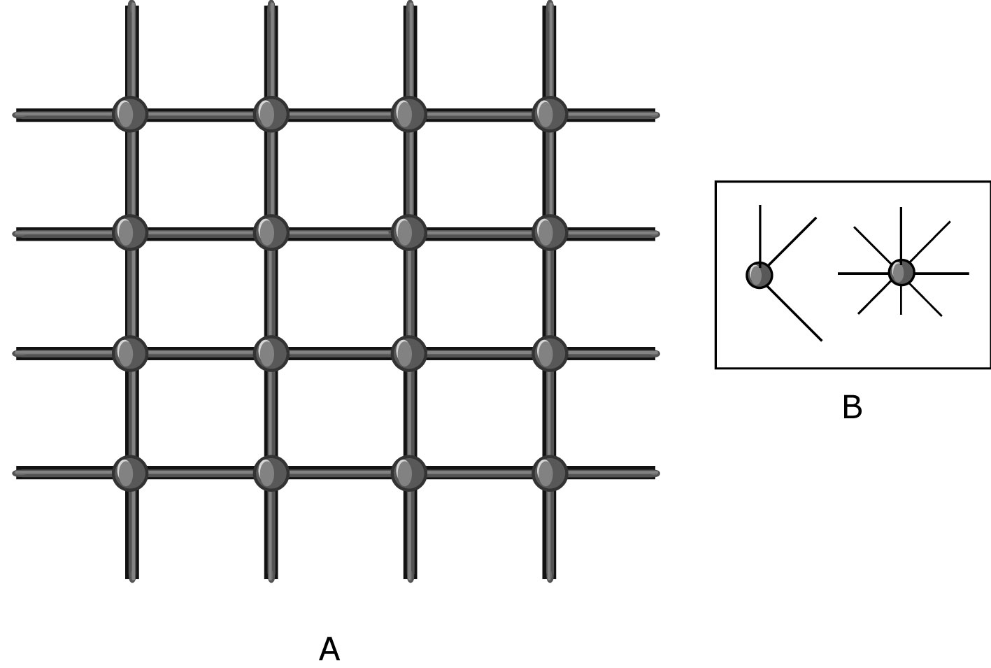
Figure 1. A network of simple processing nodes. The node connection scheme is not fixed, as illustrated by B.
The word "cell" refers to the units out of which the cell matrix hardware is made. The nodes in a network correspond to individual cells, and the network to cell interconnections. Each cell has the ability to perform simple logic functions on its inputs and produce outputs. The set of possible logic functions includes typical small-scale integration logic function: NAND, XOR, etc., as well as larger, more complex functions: one-bit full adder, two-bit multiplexer, etc. In fact, a single four-sided cell is capable of implementing over 1019 different functions of its four inputs; a six-sided cell can implement over 10115 functions.
A small memory contained within the cell is used to specify the logic function. This memory block functions like the cell’s DNA, or the machine code of a CPU, dictating the full scope of the cell’s response to inputs. The difference from DNA is that the inputs and outputs are of the same ilk (bits), and inputs and outputs are equally complex. Figure 2 shows how the memory block can be set such that the cell performs a useful operation. In this case, the cell is configured as a 1 bit full adder.
Figure 2. A cell, with the memory block enlarged and shown at the top of the figure. This cell's memory is set up to implement a One-Bit Full Adder. This D-mode cell adds A, B and C and produces S and C. The lines with arrowheads indicate wires connecting the cell to a nearby cell. Cells are connected to their nearest neighbors. In this example, to 4
neighbors. Useful work is done by the exchange of information among neighbors (in parallel).
Cells, then, act as simple logic blocks. More complex function is built up out of collections of cells. A region of a cell matrix is "configured" to behave like a specific circuit. That is, each cell’s memory block is set up to perform a subset of the larger circuit. Each cell is a node at which a small amount of progress toward a larger system/circuit is made. A small example is provided in Figure 3, which shows a set of cells that have been set up to implement a counter. The upper left corner is a cell configured to act as a crystal. This cell continuously outputs a repeating pattern of high and low bits. The 8 columns on the right are 8 toggle flip flops, each composed from three cells. The clock input is on the left of the middle cell, and the bit value is output on the right of the middle cell, as well as the top of the top cell. If the lower left cell’s bottom input is set to 1, the crystal’s bits will be directed to the clock input of the leftmost flip flop, causing that flip flop’s output value to change every other tick. Its output is also sent to the next flip flop’s clock input, causing that flip flop to toggle every fourth tick, and so on. Hence the set of outputs implements a ripple counter.
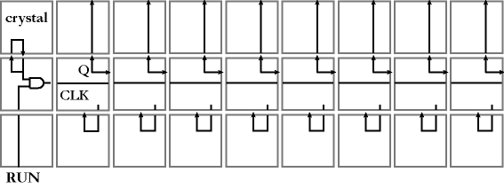
Figure 3. A simple circuit built on top of a set of 27 4-sided cell matrix cells. The circuit shown is a counter.
Cell Configuration
The next issue is how each cell comes to be a particular piece of a circuit. That is, how are cells’ memory blocks set up, or configured? If all function is represented at the cell, then the ability to configure/set up a system must also be represented at that level. This is indeed the case. Cells are dual in their interpretation of incoming information. When the cell is responding to inputs based on its cellular "configuration" or DNA, it is operating in "combinatorial mode," or data-processing mode, as a combinatorial logic block. An additional mode, called "modification mode," permits the cell to interpret incoming information/bits as new code/DNA for its memory block. Cells enter and complete modification mode through a coordinated exchange with a neighboring cell. During this coordinated exchange, a neighboring cell provides a new truth table (DNA) to the cell being modified. Thus cell configuration is a purely local operation, involving just the two cells: the cell that has the new code/DNA information, and the target cell into which the information goes. Because they are purely local, these configurations can occur simultaneously in many different regions of the matrix.
Note that every cell within the matrix is capable of operating in either combinatorial or modification mode. There is no pre-existing determination of which cells are in which modes. The mode of a cell is purely a function of its inputs from its neighboring cells. In a typical complex application, the cell matrix will contain some cells that are processing data, and others that are involved in cell modification/reconfiguration. Overall function involves close cooperation, interaction and exchange among the combinatorial mode and modification mode cells within the cell matrix.
With this simple set of behaviors, it is possible not only to do general processing using a collection of cells, but to cause cells to read and write other cells’ configuration information. This leads to dynamic, self-configuring circuits whose run-time behavior can be modified based on local events.
Cell Implementation
All of the behavior details described above can be represented with a simple digital circuit. Figure 4 shows a circuit for a cell with 4 neighbors. Note that there are different ways to design and build a cell, each of which have a different corresponding digital circuits. Figure 4 shows one particular implementation, as described in US Patent #5,886,537. Other designs are currently Pat. Pending.
Note also that the design of a cell is independent of the underlying implementation technology. For example, Drexler’s "rod logic" (Drexler, 1988), once available, would work as well as silicon for implementing a cell. Whatever your underlying technology, as long as you can build a NAND gate, memory units (which can also be built from NAND gates), and interconnections, you can build a cell matrix.
Figure 4. Schematic diagram of the specification for a cell matrix cell, showing the digital logic contained within a cell.
In all designs, the largest component is a memory block to hold the cell’s DNA/configuration information. Memory size per cell is 16x8 for 4-sided cells, 64x12 for 6-sided cells (which can be 2 or 3 dimensional physically), and, in general, (2n)x(2n) where n is the number of neighbors or sides. Besides the memory, there are a few dozen simple gates (NAND, OR, etc.) plus a few multiplexers (selectors) and flip flops (single-bit memories). The silicon chip version of a four-sided cell requires approximately 1000 transistors. At least half of those transistors are for memory.
We have built small cell matrices on silicon chips and used them for small circuits. Current silicon techniques will scale up to about 500,000 cells. Current techniques will permit a 2D configuration or a multiplanar configuration. To really get beyond what conventional architectures and circuits can do, to traverse the research frontiers that cell matrices make accessible, requires much denser manufacturing techniques than are currently available in silicon. It also would benefit from manufacturing that permits higher dimensioned cells in 3D matrices.
Simple, Conventional (Static) Circuits Built on a Cell Matrix
This section discusses the use of cell matrices as a substrate for conventionally-used circuitry. Arbitrarily complex digital logic circuits can be implemented on cell matrix hardware. Examples are state machines, CPUs and computer memories, arithmetic logic units (ALUs), floating point units (FPUs), and digital signal processors (DSPs). Just as these circuits are translated to transistor-based implementations, they must be translated to a cell matrix implementation. This process is similar to the translation of circuits for implementation using small-scale-integration parts, and is well defined. It involves first the reduction of a circuit to recognized subcomponents (AND, NAND, XOR, adders, multipliers, etc.), and then the programming of cells and sets of cells to implement and connect the subcomponents.
Two examples of translation to cell matrices are provided here. Figures 5 and 6 present a schematic for a 16 by 4 bit memory module circuit and the cell matrix implementation of the memory. Each of the components of the memory circuit are represented by one cell or a handful of cells. The extension of this memory module to a larger number of rows and bits is straightforward. Figures 7 and 8 present a second translation, from a schematic for an 8 bit arithmetic logic unit (ALU) to the cell matrix implementation of the ALU. The translation of larger circuits follows the same pattern/mechanism, simply involving more cells. A schematic diagram entry system is currently being developed at Utah State University to provide a familiar front-end to digital logic designers.
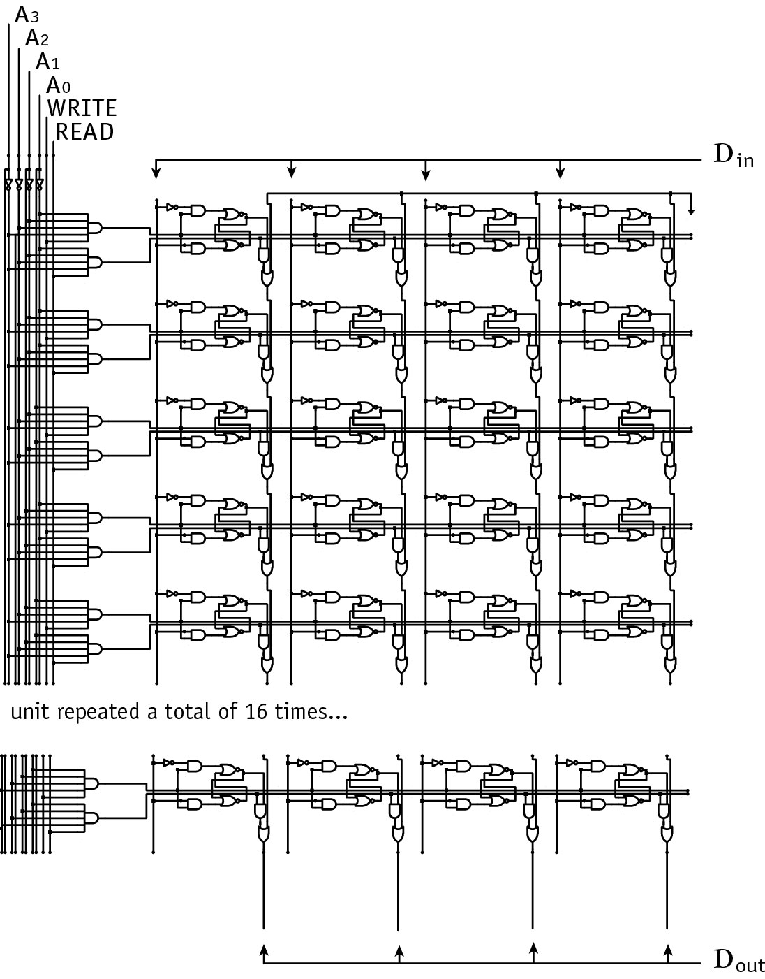
Figure 5. A schematic diagram for the digital logic contained in a 16 x 4 bit memory
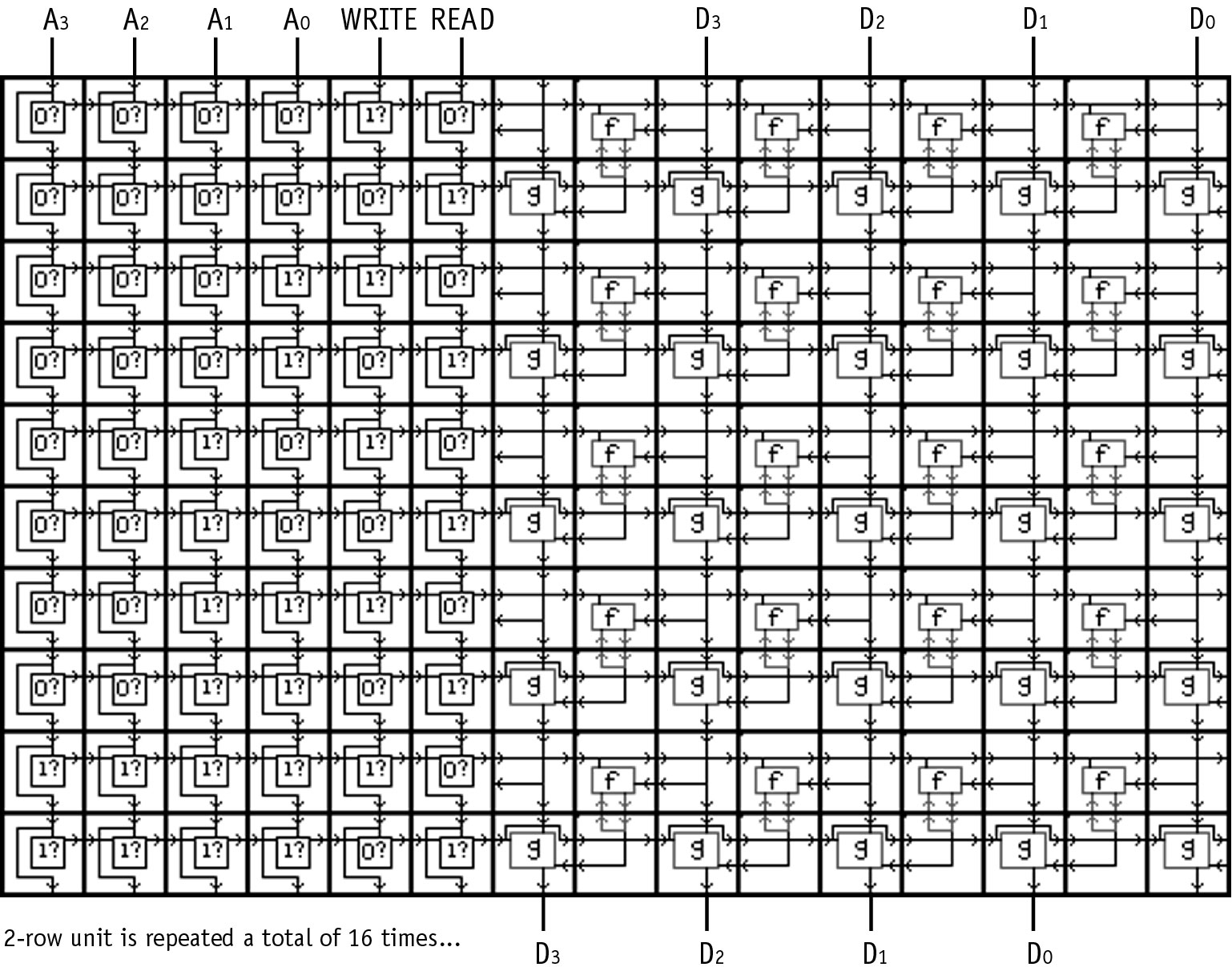
Figure 6. The schematic diagram from Figure 5, 16 x 4 bit memory, implemented on a set of cell matrix cells
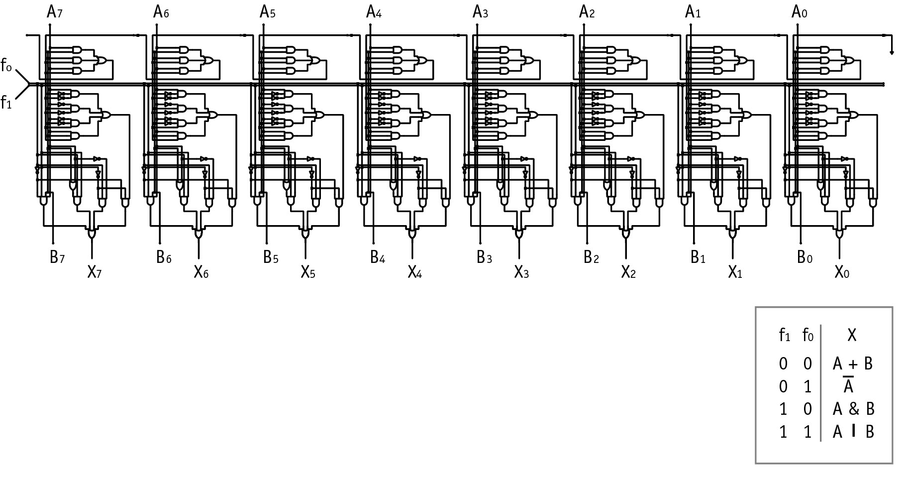
Figure 7. Schematic diagram of the digital logic for 8 bit, 4 function Arithmetic Logic Unit. The functions it performs are also shown.
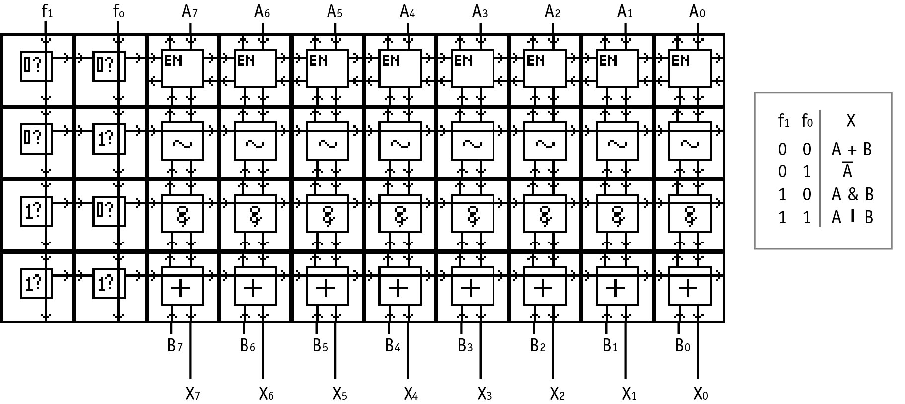
Figure 8. The schematic diagram from Figure 7, 8 bit ALU, implemented on a set of cell matrix cells
Direct translation of existing circuits does not necessarily result in the best circuit for the job, because in general, the architectures from which these circuits are translated do not exhibit the degree of distributed parallelism of the cell matrix architecture. Cell matrices can also be used to implement custom circuits that solve a specific problem faster or better than an implementation on a general-purpose machine. It is equally straightforward to use a cell matrix to implement custom circuits, given some expertise in digital logic. The custom circuit need be no more complex than the small set of problems it has to solve. Figure 9 provides an example of custom circuitry that attempts to match an input to a set of known inputs. This circuit compares an input bitstream containing an arbitrary number of bits, say n bits, to some number of possible matches, say m matches, in parallel. This circuit is nice because it is straightforward to implement, and it gives the answer in one step rather than nxm steps. In a case where n and m are large and the system is intended to do its pattern matching on a long stream of inputs, the initial effort of making a parallel custom circuit becomes preferable over running a sequential program on a general-purpose computer.
Using a cell matrix also promotes rapid prototyping and permits refinement of the circuit over time. It also permits outright changes to the circuit specification. All of these are natural uses of a hardware programming environment that improve the end result. At the end of the development cycle, the circuit can be constructed directly in dedicated hardware if desired. For conventional circuits, using conventional fabrication techniques, dedicated hardware versions will generally operate faster than a cell matrix implementation because of the repeated node delays in a cell matrix. It is currently unclear what the magnitude of these delays will be with atomic-scale manufacture; if both dedicated hardware and cell matrices fall within the picosecond delay range, the difference may be negligible or may fall within acceptable engineering limits.
Another consideration in implementing conventional circuits on cell matrices is that they can take advantage of the architecture’s natural fault isolation. The additional logic to detect and handle faults as they occur can also be added to the circuit definitions, rendering the end result significantly more robust to defects or damage than standard custom ASIC or FPGA-based systems. We are currently working toward integrating basic and not-so-basic fault detection and handling into useful circuits, and we expect to eventually make this fault handling readily usable for any circuitry.
Direct translation of existing digital circuitry is one use of the architecture, and may prove worthwhile if cell matrix manufacture becomes sufficiently inexpensive. Or, if it can be used to easily add a beneficial feature to the system, such as fault tolerance, then use of a cell matrix may be preferred over custom ASIC or FPGAs. Another feature of the architecture is rapid configuration times due to the ability to configure many regions of a matrix at once. Even with today’s silicon technology, configuration times for FPGAs are not as short as one would like. Rapid configuration increases in importance with hardware platform size, and becomes tantamount to success with trillion trillion switch systems (as does fault tolerance).
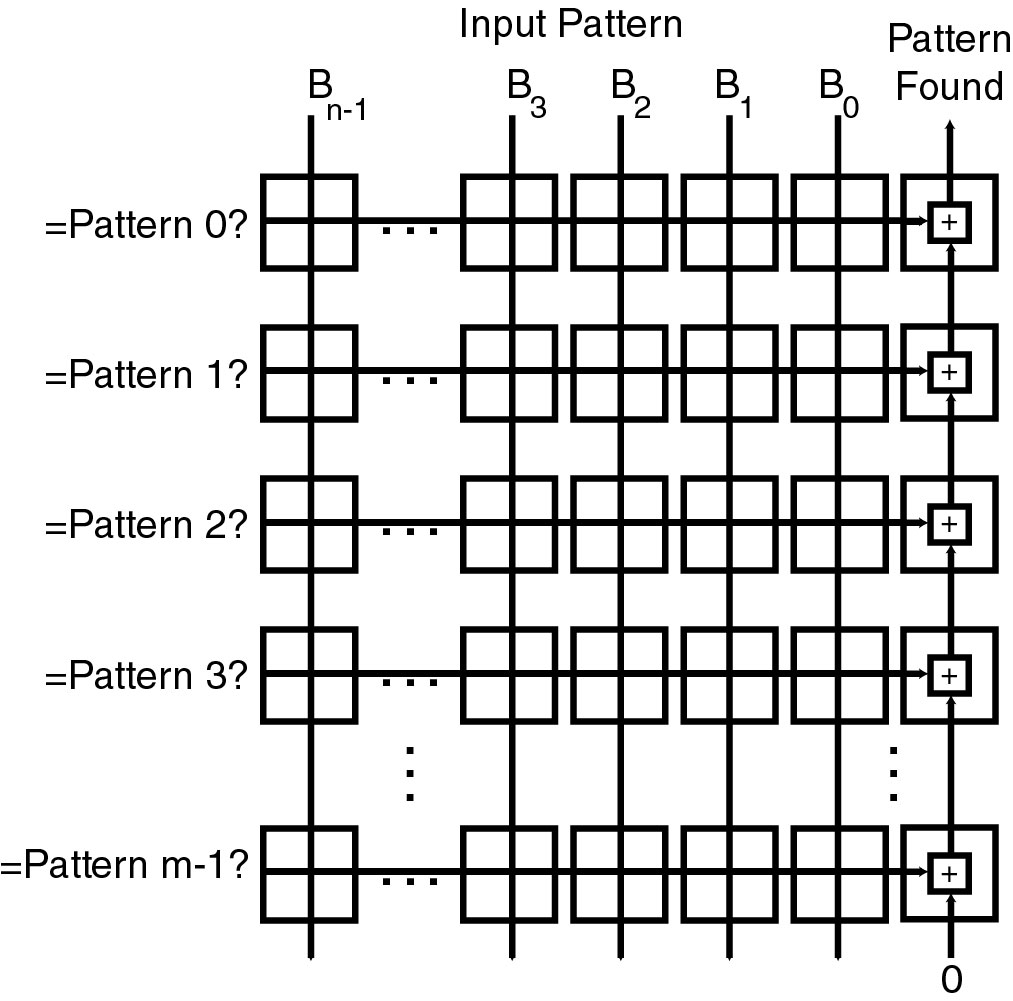
Figure 9. This circuit tests an n-bit input pattern B against m different test patterns. Each row j is configured to compare all n input bits, in parallel, with the n test bits of pattern j. All m patterns are checked simultaneously. Thus all m x n comparisons are performed in a single time step.
Dynamic, Self-Modifying Circuits on a Cell Matrix
Conventional circuitry is largely static: the hardware configuration does not change during its use. Cell matrices can implement static circuitry, as shown in the previous section; however, they can also implement dynamic circuitry. This section describes the benefits of dynamic circuitry and some important architecture characteristics that make dynamic circuits convenient enough to become a commonplace tool for problem-solving, as well as a critical element in extremely large systems.
Simply put, dynamic circuits change during their execution. For example, in dynamic circuits, cells or networks of cells might change behavior, or they might change the behavior of regions around them, or they might migrate to new positions in the matrix, or shrink, or expand to include more cells. These changes can be designed to occur in a deterministic and orderly progression, such as the design of expanding counters or multipliers which extend themselves to avoid an arithmetic overflow condition. Or, the changes can be nondeterministic in nature, as might be useful in certain evolvable hardware experiments, or outside of programmer knowledge/control, such as onboard automatic system optimization or repair.
An example in which dynamic circuit reconfiguration could improve system function is found with arithmetic logic units used by CPUs to perform a set of basic instructions such as addition or logical negation. ALUs do not contain dedicated circuitry for all arithmetic functions, just for a limited set, the set being determined (and forever fixed for the life of the system) by the hardware designer by analysis of a set of "typical" problems. When a function from the short list is encountered, it is handled efficiently; the rest are handled more slowly, by a series of operations.
In a cell matrix, dynamic components of the circuit could be used to improve ALU function on a per-problem basis. A (static) monitor could observe the instructions being executed by the CPU, including the ones which can be performed directly by the ALU and those that require a series of ALU operations. The monitor would compile statistics on the most heavily used functions over a period of time. If this list fell too far out of line with the current list of ALU functions, the monitor would initiate the synthesis of a new ALU which would include the more heavily used functions, while eliminating the lesser-used ones. The new ALU, once constructed, would then be swapped in by changing a single routing path switch. The next subsequent ALU synthesis would then be performed on the former ALU, and so on. Making the ALU dynamic would, in effect, permit the on-the-fly optimization of the ALU to the problem currently being solved. On a cell matrix, it is also important to note that the operation of the monitor and ALU synthesizer would not slow down the overall system function; they would operate in parallel, using their own resources, separate from the CPU/ALU and the rest of the system, and separate from any other systems currently running inside the cell matrix.
Dynamic circuits are also useful in the detection, isolation, and handling of faulty cells. For example, it is possible to build a circuit which perform the equivalent of a "scandisk" operation on hardware. Such a circuit would perform an initial analysis of an empty cell matrix, testing different regions of the matrix (in parallel), and looking for faulty cells. Once detected, faulty cells would be isolated by good cells around them, and markers would be placed to indicate the location of these bad cells. Future configurations would then look for these markers before using a region in side the matrix.
Dynamic circuits can also be used to support run-time fault tolerance, by configuring empty regions of the matrix to replicate circuits occupying recently-failed regions. Once the circuits have been replicated, the interconnecting pathways between circuits would be rebuilt, to map in the new circuits and remove the old.
For hardware that must be configured, internal, distributed, local system modification is a fundamental requirement for trillion trillion switch systems. More generally, for both configurable and nonconfigurable trillion trillion switch systems, internal, distributed, local system control is a fundamental requirement. External and/or nonparallel control or modification would grievously impare system throughput, rendering such large systems uselessly slow.
Part 2: Efficient Utilization of Extremely Large Numbers of Switches
The cell matrix architecture’s support of distributed computation and distributed control and its natural parallelism provide a good platform for the development and use of extremely large circuits, such as those which may be possible using atomic-scale manufacturing. This is demonstrated here by example. In this example, a large search space is efficiently searched, first by laying down a grid of custom processors on the matrix, each of which is responsible for a small subset of the overall space, then by the propagation of a small set of input data to all processors in parallel in an advancing front style, then by processors’ execution of a simple pattern matching algorithm, all in parallel, then by the propagation of the "right answer" to a corner of the grid.
This basic technique is used here to construct a fast circuit for discovering the key which was used to encrypted text using the 56-bit Data Encryption Standard (56-bit DES) (NIST, 1993). Such a key search is sometimes referred to as "cracking." Cracking 56-bit DES is a good choice among search space applications because:
- it truly requires an exhaustive search: there is no way to prune the search space or creep up on the solution iteratively. This makes it a naturally large problem, yet
- it can be accurately modeled by a pared down data encryption scheme, such as a 4-bit DES, and thus the solution mechanism can be built and tested using conventional hardware.
Design of a 56-Bit DES Cracker
The DES cracker uses a 2D or 3D grid of individual processors. Figure 10 shows the basic design for a single processor. Cracking requires two things: a piece of unencrypted text, called plain text, and the corresponding encrypted text, called cipher text. The object of each processor is to encrypt the plain text using one particular key, and then compare the result to the "desired" cipher text. If the result matches the cipher text, then this processor must have used the right key. The key is then passed out of the processor to a fixed location in the matrix, from where it can be presented as the final output of the machine. The "SEND" block and the "Match KEY" signal are used in this process, which is more fully explained below.
Each processor contains several distinct blocks of circuitry. These are represented in Figure 10 as a vertical series of black boxes that compute something and pass a result along to the next box downstream. The first block, labelled "MyID" in the figure, receives unique positional information while it is being configured, such as the processor’s row and column in the overall network. This information is passed to the "genKEY" block, which uses it to construct a unique key. This key is a candidate, one which may or may not correctly encrypt the plain text into the encrypted text. The full set of possible keys is represented by the full set of processors in the network represented in the figure. The block labelled "Match?" takes the key from genKEY and encrypts the plain text using its key and the known DES algorithm. It then compares the result to the cipher text, i.e., the proper encryption of the plain text. If the cipher text does not match the locally-encrypted text, then the match failed, and the Match? block sends a zero to the block labelled "SEND."
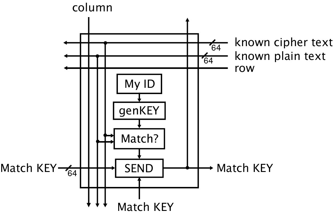
Figure 10. Diagram of a single processor for the DES Cracker
Figure 11 shows the design for processor communication, as well as the larger algorithm that the circuit implements. Processor communication is handled largely by the SEND signal that is the result of the SEND function performed by each processor. The inputs to all processors are the cipher text and plain text, which are put in at the upper right corner of the network. The wires shown in the figure represent busses, or sets of wires; the number of wires per bus are indicated. Keep in mind, these wires themselves are built from cell matrix cells. There are no underlying communication pathways available within the cell matrix other than between neighbors. Sets of neighboring cells act cooperatively to function as wires and buses.
Signalling occurs asynchronously, and the time to propagate the inputs is a simple function of propagation delay. The time to propagate the Match KEY signal is also primarily a function of propagation delay (and also depends, less significantly, on the time it takes one processor to compute its SEND signal). The processors operate independently and in tandem. When the system starts, all processors begin outputting zeros for their Match KEY signals. As soon as a processor has computed its match signal, it updates its SEND signal based on whether or not it matched. The SEND signal is computed all the time, not just once; asynchronously with the processor’s computation of its own match signal, its SEND block is receiving results from the processors to its left and below it. The network is given an opportunity to settle its outputs, long enough that all processors have computed their match signals and have propagated their results to the upper right corner of the circuit. At this point the right key is sampled from the Match KEY signal at the upper right corner of the circuit, and the answer is thus obtained.
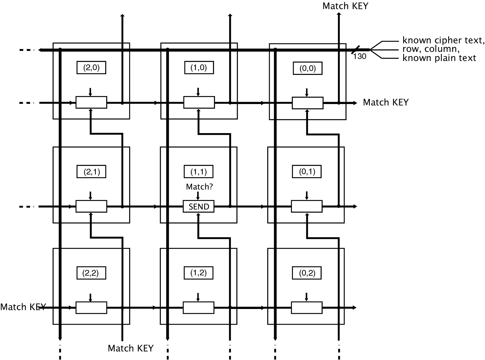
Figure 11. Network Diagram for a 56-bit DES Encryption Cracker Utilizing A Spatially Distributed Parallel Algorithm. This diagram shows how the processors communicate with each other. Only 9 of the processing blocks are shown
The SEND signal is a locally computed signal that gets summed up across the grid to provide an answer at the upper right corner of the circuit. Interprocessor communication is limited to this simple, monotonically moving signal. If any processor’s key matches, it passes its key to those processors it communicates with, i.e. the processor above it and the one on its right. They in turn pass the key onward to all the cells above them and to the right of them, and so on, through all processors that lie above and to the right of the match, until the key reaches the upper right corner of the circuit. This can be thought of as the match key being percolated upward and rightward until it reaches the destination. Because this is hard to picture or represent in a static image, a simulation of this process is provided on our Web site, www.cellmatrix.com, and you can observe the wavefront or percolation process and set the match point to whatever processor you like.
|
Left |
Below |
Match? |
SEND |
|
Y |
- |
- |
LeftKEY |
|
- |
Y |
- |
BelowKEY |
|
N |
N |
Y |
self KEY |
|
N |
N |
N |
0 |
Table 1. Logic Table for SEND signal. "Y" indicates a matched key is available from the left, from below, or from the current processor. "N" indicates such a key is not available. "-" is a don’t care. SEND column indicates which key is output by the processor (0 means no key is sent).
Design Implementation
This section addresses the construction of the DES cracker, i.e., the layout of the processors and interconnections onto a cell matrix. Constructability in parallel is one of the initial considerations during the design of the DES cracker (and of any of the class of spatially distributed circuits it represents). The construction algorithm and mechanism described here grows as the cube root of the number of processors in 3D, and grows as the square root of the number of processors in 2D. These times are achieved by taking advantage of the architecture’s parallel, distributed control.
It is important for the circuit design to be one that can be laid down on a cell matrix in parallel, under matrix control. To this end, the assignment of keys must be sufficiently programmatic that it can be easily automated, and so that it does not require that the processors themselves be different from each other. We achieve this by designing the processors such that they generate their own keys based on positional information determined at run time. Although they later use their positional information to construct different keys, the processors themselves are identical to each other. This makes it possible to quickly lay down identical processor configurations in parallel throughout the matrix, which then differentiate to represent the full set of possible keys. If insufficient hardware is available to dedicate each processor to a single key, the process is the same, except that base keys, which differ by some number "d" are distributed among the processors, and each processor generates d keys from the base key it receives. The logic blocks that generate and compare the keys are also modified to check all d keys for a match.
Figure 12 illustrates the wavefront-style algorithm used to populate a cell matrix with DES cracker processors. The squares represent regions, blocks of cells, large enough to contain a processor, its interconnect, and any configuration circuits needed to implement local configurations. The algorithm is recursive. A region in the upper right corner of the circuit is configured with an intermediate configuration. This configuration permits it to configure the regions to its left and directly below it. Each of these regions is provided with an intermediate configuration that permits them, in turn, to configure the regions to their East and South with an intermediate configuration that permits the third tier to configure the fourth tier, and so on. The tiers correspond to generations, one new generation spawned per time step. Tier membership is indicated by shading in the Figure 12 A, with the processors belonging to each generation shown by lines in Figure 12 B.
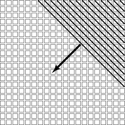
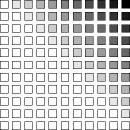
Figure 12. Two images of the procession of a wavefront-style configuration from the upper right corner outward
Using this configuration strategy, (n2+n)/2 processors will have been configured by generation n. On a three-dimensional matrix, the number of processors configured by generation n is on the order of n3. In this way, the 72,000,000,000,000,000 processors required for 56-bit DES can be configured in under 417,000 generations.
The algorithm assumes that the only area of the matrix to which it has access is the upper right corner. If more points of entry are available, or if the center of the region is accessible, then the algorithm could be modified to take advantage of accessibility to cut configuration time further.
4-bit DES Cracker
Current simulation and fabrication techniques make the construction or simulation of the full 56-bit system difficult, on account of the costs—the cost of hardware for the physical implementation and of CPU time for the simulations. Therefore a much smaller circuit was designed and tested. We used the specifications for 56-bit DES to design a similar but smaller 4-bit DES, and then constructed a simulation of a 2D grid of 4-bit DES cracking processors. The circuit employed in the 4-bit version is perfectly scalable, and can easily be augmented to represent the full 56-bit DES algorithm.
Enough text must be provided to the machine such that only one unique key correctly encrypts the text. Insufficient amounts of text cause more than one key to match. With only 4 bits in the key, and only 4-bit text strings, many overlapping keys were encountered. This issue can be handled either by enlarging the text busses to provide a longer text string or by introducing extra logic into the processors such that the system can iterate on small text strings until the unique, correct key is established. This second approach was taken in the 4-bit DES cracker built to test the machine design. This approach requires that each processor maintains a single piece of information, namely, whether the key has successfully matched all substrings of the text. A flip flop was added to the processor to maintain this one bit of state information, and some additional logic was added to correctly set this signal. State information requires some synchronization so that cells properly set and read their states. This synchronization is accomplished by two extra input signals added to the basic design, as shown in Figure 13. The init input signal indicates to the processor that it should clear its state bit; the strobe signal is used to tell the processor to perform the "Match?" function. The strobe signal ensures that the comparison between cipher text and plain text will not occur until both text inputs are in step and valid to compare.
A cell matrix implementation of the processor design is shown in Figure 14. Each processor takes about 2,500 cells; the circuit could have compacted, but was instead built in a scalable fashion. No advantage was taken of any particular aspects of the algorithm. For example, if a 4-bit permutation only involves swapping two bits, a full 4-bit permutation block was still built. Therefore the circuit is laid out as if it were a 56 or 64 bit circuit, and enlarging it is a straightforward process. The 4 bit DES circuit was tested on a cell matrix simulator that runs on a desktop PC. The circuit was tested with a range of key values and text strings to ensure that both the processor design and its implementation were correct.
It is interesting to observe the signalling that occurs during the circuit’s operation, and the parallel operation of the processors becomes evident to the viewer. An animation generated from screen captures is available on our Web site, www.cellmatrix.com
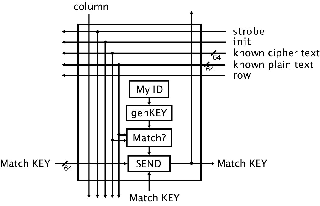
Figure 13. The processor implemented for the 4 Bit simulations
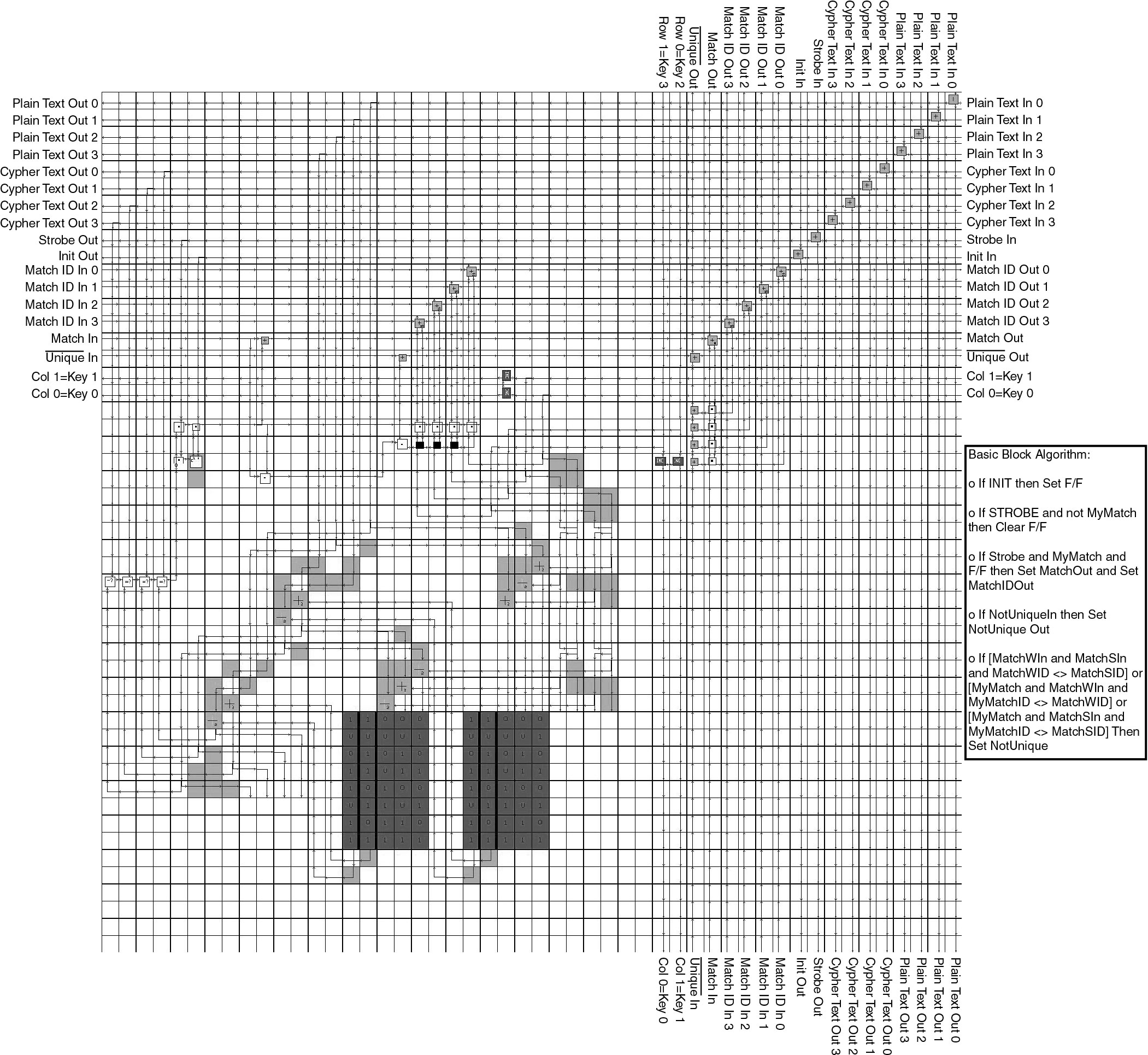
Figure 14. Implementation of 4 bit Key Finder processor on a cell matrix
Performance and Costs
The chief cost for the DES cracker is not time, as it is with CPU/memory architectures. Instead the chief cost is hardware. The point of spatially distributed algorithms is to efficiently "throw hardware" at a time-consuming search space problem by breaking it down into smaller tasks performed in parallel over a large cell matrix. Overall circuit size is dictated both by the problem size and the amount of hardware available. For 4-bit long keys, there are 24 possible keys, and a 2D configuration of processors is only 4x4. For keys that are 56 bits long, there are 256 possible keys. Representing all keys at once, one per processor, takes about 1017 processors. In a 3D configuration, the sides of a cube that contain all 1017 processors is just under 417,000 processors wide in each direction. Each processor requires about 4 million cells, resulting in a total of roughly 3x10²³ cells in the full 56-bit machine. Note that this number is a maximum, in that it assumes that each processor handles only one key.
The algorithm and circuit design presented here achieves the minimum run time possible, O(1), which is to say that it takes a constant amount of time to determine the key. The actual time required depends on two components. First is the time required for one processor to test its unique key. The DES algorithm, as implemented here, involves no looping. It is a purely combinatorial circuit. The plain text and key go into one end, and the encrypted text comes out the other. Its execution time is thus a pure function of propagation delay. For a single 56-bit DES processor, organized in a 160x160x160 cube of cell matrix cells, the total path length from input to output might be approximately 32,000 cells. Therefore, if the propagation delay from cell to cell is t, the total time to encrypt one block of text (56 bits, or 8 characters) would be 32000*t.
This is likely a negligible amount of time, compared to the second factor in execution speed, which is the total propagation delay throughout the network of individual processors. A 3D 56-bit machine is a cube with 417,000 processors on each side. Each processor is 160x160x160, so the total size of the cube is 66,720,000 cells per side. The longest path through the cube is from one corner to the other, which traverses the width of the cube three times (once in each direction), and thus passes through roughly 200 million cells. Assuming a one picosecond propagation delay from cell to cell, this corresponds to 200 microseconds. This means 5,000 blocks of text can be processed (i.e., cracked) per second. Each block contains 8 characters, so this amounts to 40,000 characters per second, sufficient for analyzing text transmitted at 256K baud.
Configuration time must also be considered, since the DES cracker circuit must first be set up on the hardware. Computing actual configuration time depends heavily on the underlying technology: how fast circuits can be clocked, how stable the clocking is, and so on. However, it is useful to compare orders of magnitude. For the purpose of discussion, assume a single DES processor (which tests a single key) can be configured in 10 microseconds. Because of the ability to build circuits in parallel, this time also represents the time to build each generation of processors. Since all 256 processors can be configured in only 417,000 generations, the entire machine can be configured in under 5 seconds. Remember, this is a one-time cost. Once you’ve configured the machine, it then operates at a much higher speed (256K as described above). In contrast, on a sequentially-configured system, such as an FPGA, assuming the same 10 microsecond configuration time per processor, configuring all 256 processors would require more than 22,000 years.
Summary
On a cell matrix, the algorithm and machine can be constructed to efficiently distribute a search space over a large number of custom processors. The construction of all the processors can be done in parallel (efficiently) on a cell matrix. Processor network topology and interprocessor communication can be hand-crafted. Note that these are not general purpose CPUs, but are simple, special-purpose processors that are designed specifically for this algorithm. They do not receive instructions to execute, as CPUs do; rather, they are hardwired to execute their specific function as quickly as possible.
This solution is also quite flexible. If 1023 cells are not available, then the same algorithm can be run on a smaller number of processors, where each processor is responsible for a set of possible keys rather than a single key. The algorithm is still O(1), although the constant factor is larger.
This solution can also be adapted to work on partially-faulty hardware. Faulty blocks can be detected and avoided during configuration, and dynamic key assignment during configuration can be made to take into account missing blocks. Transmission of information throughout the machine is already redundant by design, and in general, a missing block will not prevent nearby blocks from receiving or transmitting within the network.
The spatially distributed circuit and algorithm described here for DES cracking appears to be a good general approach to large search space problems. The approach is applicable elsewhere, to many different problems. Coupled with a method for fabricating extremely large cell matrices, these circuits will greatly improve upon the solution times for very large search space problems. They also provide a good application for trillion trillion switch computing, and an additional motivation for the fabrication of the cell matrix architecture, in that what they do is not possible on conventional computers.
In the case of the 56 bit DES cracker presented here, the circuit roughly corresponds to a multiple instruction, single data (MISD) computing architecture, which until now has mostly been a theoretically useful construct with no concrete examples (Chalmers, 1996). The plain and cipher text are the single data, and the processors perform the multiple instructions, in that each processor interprets the data differently, based on its internally-generated key. The MISD analogy appears to hold for only a subset of spatially distributed circuits, because the processors used need not be identical, but they need to be easy to differentiate in parallel during system configuration so that system configuration is not expensive.
Conclusions/Discussion
This paper presents the structure and function of the cell matrix architecture in terms of its applicability to nanocomputing. The architecture is structurally simple but as computationally complex as is required by the problem being solved. The physical hardware is fixed, and its function is specified by configuring memory held at each hardware node. Examples are provided to demonstrate the wide range of circuits that can be built on a cell matrix, and to show that it is a small leap from a schematic diagram to a cell matrix configuration.
The cell matrix architecture has many benefits. It is easier to manufacture than other computing architectures because of its completely regular structure. It is easier to use than cellular automata, faster to configure than FPGAs, more scalable than FPGA or CPU/memory architectures, and it is inherently fault tolerant.
The applicability of the architecture to the huge switch counts that atomic-scale fabrication will eventually provide is also explored. This applicability arises out of the architecture’s distributed, local, parallel control. A circuit is presented which appears to successfully organize about 1026 switches into an O(1) searcher. This fast circuit was achieved by the development of what we term spatially distributed algorithms and circuits. These circuits take advantage of inherent properties of the architecture to customize the hardware and to do so efficiently.
Future Work
The DES cracking application presented here is just one example of what is actually a wide variety of exciting research that one can undertake with this architecture. A similar style of circuit is currently being developed for quickly finding the root of a function of the form f(x) = n. We continue to work toward making cell matrices more widely accessible to more people for more problems by developing tools, methodologies, supporting circuits and cell libraries. We also continue research in useful applications of dynamic circuits and the architecture’s ability to examine and modify itself. In particular, we see a need for distributed, local fault handling so that extremely large systems can successfully run despite faults. The relative importance of fault handling will increase dramatically with the increased rate of fault occurrences in trillion trillion switch systems. To begin to address this we are developing onboard autonomous fault detection and repair that takes advantage of available undamaged cells. A larger goal is a general strategy and encapsulated circuitry so that all large circuits can easily incorporate fault tolerance.
There are many other interesting research areas to which this architecture can be applied. One general area involves the development of ideal circuits for problems that are time-consuming on conventional hardware such as operations on large matrices, wide bit arithmetic, and simulations of complex, 3D phenomena. The usefulness of the cell matrix architecture in the field of Evolvable Hardware, where circuits are dynamically constructed and modified using a genetic algorithm approach, has been suggested by researchers in that field (de Garis, 1999: Miller, 1999). A sample application of the cell matrix to this field is given in (Macias, 1999). Current research in brain building is also likely to benefit from the architecture’s unique self-modification and support of internal monitoring. A good deal of research in self-organizing, self-optimizing systems is also possible using this architecture, and we have barely scratched the surface of this potential.
References
Bishop, F., "A Description of a Universal Assembler," Proceedings of the IEEE International Joint Symposia on Intelligence and Systems , November 4-5, 1996, Rockville. MD.
Chalmers, A. and Tidmus, J., "Practical Parallel Processing," Thompson Computer Press, 1996.
Collier, C. P. et al., "Electronically Configurable Molecular-Based Logic Gates", Science ,1999 July 16; 285: 391-394.
de Garis, H., "Review of Proceedings of the First NASA/DoD Workshop on Evolvable Hardware," IEEE Transactions on Evolutionary Computation , Vol. 3, No. 4, Nov. 1999.
Drexler, K. E., "Rod Logic and Thermal Noise in the Mechanical Nanocomputer," Molecular Electronic Devices , F.L. Carter, R. Siatkowski, H. Wohltjen, eds., North- Holland 1988.
IBM, "Blue Gene to Tackle Protein Folding Grand Challenge," http://www.no.ibm.com/nyheter/des99/bluegene.html, 2000.
Joy, B., "The Future of Computation," Papers from the First Foresight Conference on Nanotechnology , BC Crandall and J. Lewis, eds., 1992.
NIST, "Announcing the Standard for DATA ENCRYPTION STANDARD (DES)," Federal Information Processing Standards Publication 46-2 , December 1993.
Macias, N, "Ring Around the PIG: A Parallel GA with Only Local Interactions Coupled with a Self-Reconfigurable Hardware Platform to Implement an O(1) Evolutionary Cycle for Evolvable Hardware," Proceedings of the 1999 Congress on Evolutionary Computation, 1999.
Mead, C., Comments made during the 2nd NASA/DoD Conference on Evolvable Hardware, Palo Alto, CA, 2000.
Miller, J., "Review: First NASA/DOD Workshop on Evolvable Hardware 1999," Genetic Programming and Evolvable Machines 1 , A. Stoica, D. Keymeulen and J. Lohn, eds., pgs. 171-174 2000.